ESI has been in business since 1986 working with Plasma Etchers and Ashers. Offering services and technical support in Semiconductor, MEMS, Biomedical, Nanotechnology & LED industries. We have become the industry leader in remanufactured Gasonics L3510 Asher equipment.
To achieve this, we have been providing unique innovative upgrades and cost-effective technical solutions, high-quality equipment, and on-time spare parts delivery worldwide. We have maintained a global presence that has grown and expanded into the major high-tech manufacturing areas of the world.
ESI’s experienced engineer team is the best guarantee for high-quality service and support. We provide on-site installation, training, maintenance, system optimization, retrofits, and customized upgrades.
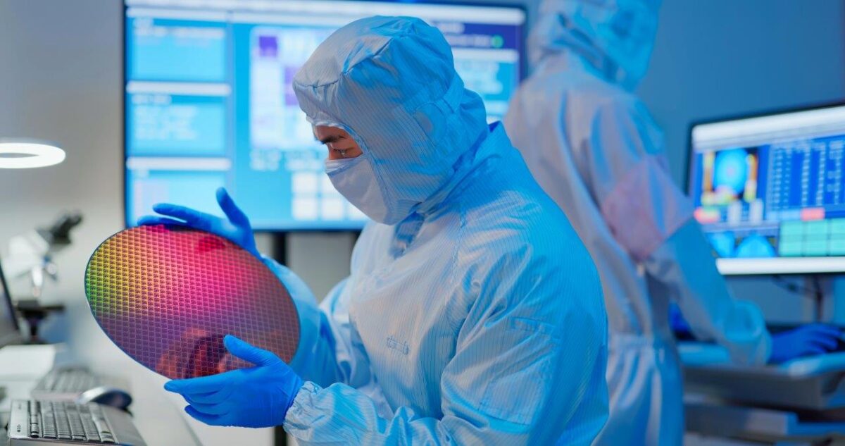
We manufacture and test all our products in our Class 100 certified cleanroom.
The ESI e3511, e105, e106, e303, e590, e490 were developed to replace these older obsolete product lines with new PC, Software and robotics but still process compatible. This reduces customer product qualification time required for new process-based tools.
The New ESI developed e3611and 3612 Plasma Ashers bring High Throughput and Low Cost of Ownership with Small Footprint
Browse our full range of product & support, or ask our experts to find the perfect model for your application
e3611/e3612 Single Wafer Ashing Systems
Advanced Single Wafer Plasma Asher
Process Definitions
Ashing: Stripping the photoresist. Typically performed after ion implantation or etching.
Descum: Removing remaining photoresist or polyimide on wafers for front-end, removing a small portion of resist on the wafer.
Etching: Isotropic etch for materials such as Si3N4, SiO2, and Poly-Si
Surface Treatment: Surface activation before wet etch to improve etch process step, improves surface adhesion enhancement before deposition.
Cleaning: plasma cleaning could be performed after wet etch to complete the cleaning step or after DRIE to remove polymer from the via etc.
Applications
Bulk Resist,
Post LDI Resist Strip
Polymer Removal
Descum processing
Surface Treatment for better Dep Adhesion
Post high dose implant strip
Oxidation
Isotropic etch
MEMS
Features
TCP 6KW RF plasma or 3KW Microwave Plasma
Compact Footprint, Very Low Cost of Ownership
Single or Dual Arm Pick and Place Robot
Downstream Plasma for extremely low damage
High throughput >100 wph
Dual Cassette Holders for 100mm to 200mm wafers
Optional SMIF Load Stations
Ethernet Smart Controls for subsystems
Cooling Stations
ULPA or HEPA System
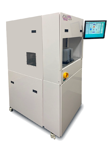
e3611
One Chamber
2 Cassette Stations
Single Arm Robot
Low COO
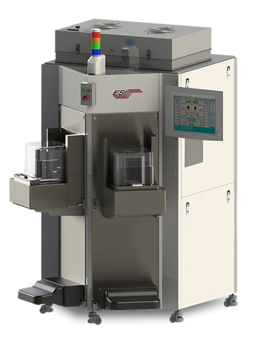
e3612
Two Chambers
2 Cassette Stations
Dual Arm Robot
Low COO